How are microprocessors made?
I found this a while ago on the 'Net, and decided to copy it over here: links die, and I wanted to keep this for Future Generations. Both text and pictures are originally from Intel.Introduction
It starts with sand
With about 25% (mass) silicon is — after oxygen — the second most frequent chemical element in the earth’s crust. Sand — especially quartz — has high percentages of silicon in the form of silicon dioxide (SiO2) and is the base ingredient for semiconductor manufacturing.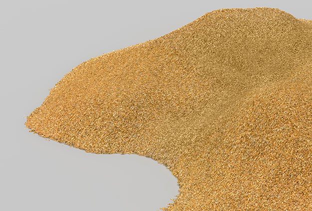
Melted Silicon
scale: wafer level (~300 mm / 12 inch)
Silicon is purified in multiple steps to finally reach semiconductor manufacturing quality which is called Electronic Grade Silicon. Electronic Grade Silicon may only have one alien atom every one billion Silicon atoms. In this picture you can see how one big crystal is grown from the purified silicon melt. The resulting mono crystal is called Ingot.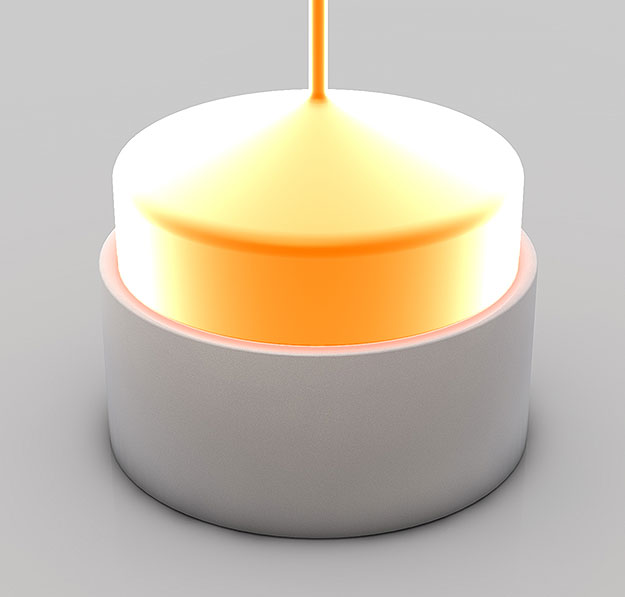
Mono-crystal Silicon Ingot
scale: wafer level (~300 mm / 12 inch)
An ingot has been produced from Electronic Grade Silicon. One ingot weights about 100 kilograms and has a silicon purity of 99.9999%.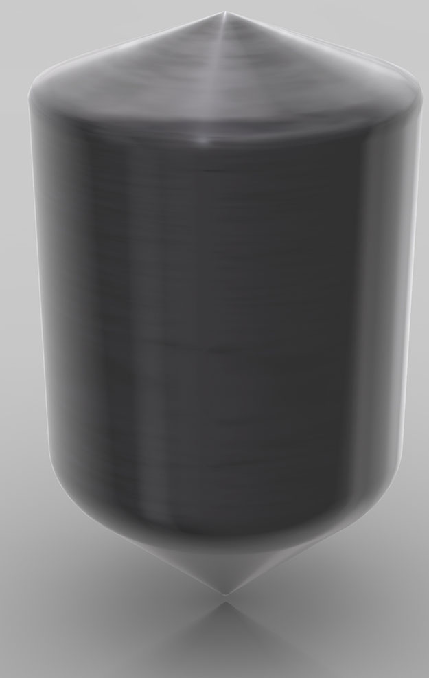
Slicing and dicing
Ingot Slicing
scale: wafer level (~300 mm / 12 inch)
The ingot is cut into individual silicon discs called wafers.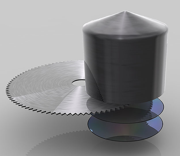
Wafer
scale: wafer level (~300 mm / 12 inch)
The wafers are polished until they have flawless, mirror-smooth surfaces. Intel buys those manufacturing ready wafers from third party companies. Intel’s highly advanced 45nm High-K/Metal Gate process uses wafers with a diameter of 300 millimeter (~12 inches). When Intel first began making chips, the company printed circuits on 2-inch (50mm) wafers. Now the company uses 300mm wafers, resulting in decreased costs per chip.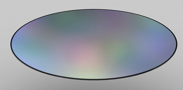
Applying Photo Resist
scale: wafer level (~300 mm / 12 inch)
The liquid (blue here) that’s poured onto the wafer while it spins is a photo resist finish similar as the one known from film photography. The wafer spins during this step to allow very thin and even application of this photo resist layer.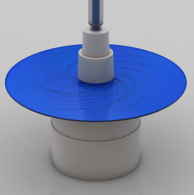
Exposing the chip
Exposure
scale: wafer level (~300 mm / 12 inch)
The photo resist finish is exposed to ultra violet (UV) light. The chemical reaction triggered by that process step is similar to what happens to film material in a film camera the moment you press the shutter button. The photo resist finish that’s exposed to UV light will become soluble. The exposure is done using masks that act like stencils in this process step. When used with UV light, masks create the various circuit patterns on each layer of the microprocessor. A lens (middle) reduces the mask’s image. So what gets printed on the wafer is typically four times smaller linearly than the mask’s pattern.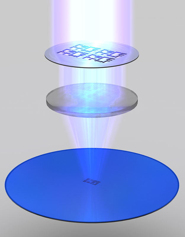
Exposure
scale: transistor level (~50-200 nm)
Although usually hundreds of microprocessors are built on a single wafer, this picture story will only focus on a small piece of a microprocessor from now on –on a transistor or parts thereof. A transistor acts as a switch, controlling the flow of electrical current in a computer chip. Intel researchers have developed transistors so small that about 30 million of them could fit on the head of a pin.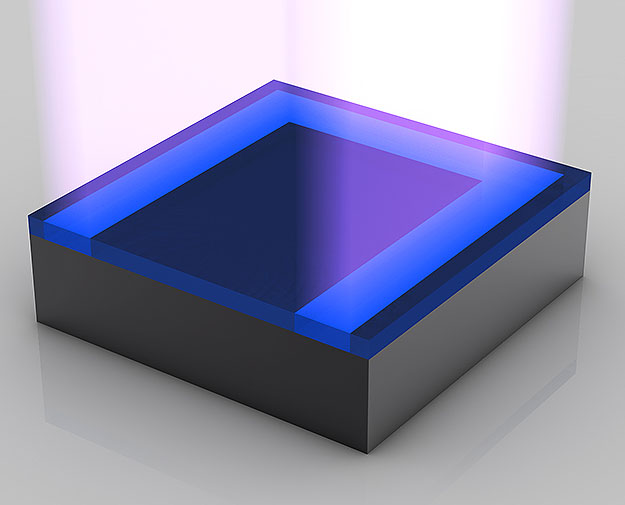
Washing off of Photo Resist
scale: transistor level (~50-200 nm)
The gooey photo resist is completely dissolved by a solvent. This reveals a pattern of photo resist made by the mask.
Etching the chip
Etching
scale: transistor level (~50-200 nm)
The photo resist is protecting material that should not be etched away. Revealed material will be etched away with chemicals.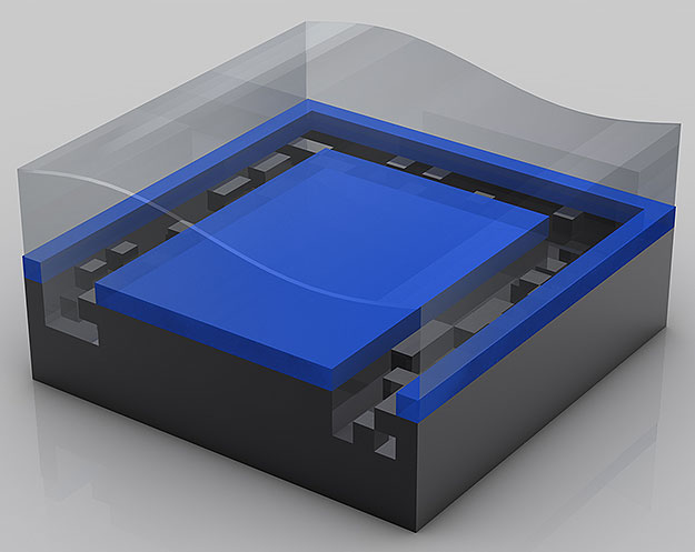
Removing Photo Resist
scale: transistor level (~50-200 nm)
After the etching the photo resist is removed and the desired shape becomes visible.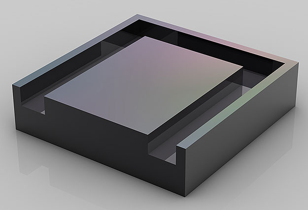
Applying Photo Resist
scale: transistor level (~50-200 nm)
There’s photo resist (blue color) applied, exposed and exposed photo resist is being washed off before the next step. The photo resist will protect material that should not get ions implanted.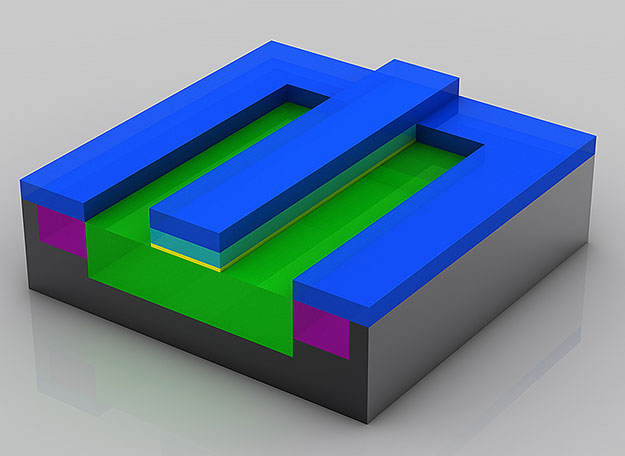
Bombarding with ions
Ion Implantation
scale: transistor level (~50-200 nm)
Through a process called ion implantation (one form of a process called doping), the exposed areas of the silicon wafer are bombarded with various chemical impurities called Ions. Ions are implanted in the silicon wafer to alter the way silicon in these areas conducts electricity. Ions are shot onto the surface of the wafer at very high speed. An electrical field accelerates the ions to a speed of over 300 000 km/h (~185 000 mph)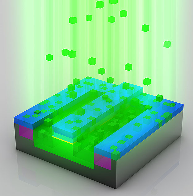
Removing Photo Resist
scale: transistor level (~50-200 nm)
After the ion implantation the photo resist will be removed and the material that should have been doped (green) has alien atoms implanted now (notice slight variations in color)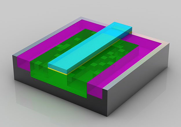
Ready Transistor
scale: transistor level (~50-200 nm)
This transistor is close to being finished. Three holes have been etched into the insulation layer (magenta color) above the transistor. These three holes will be filled with copper which will make up the connections to other transistors.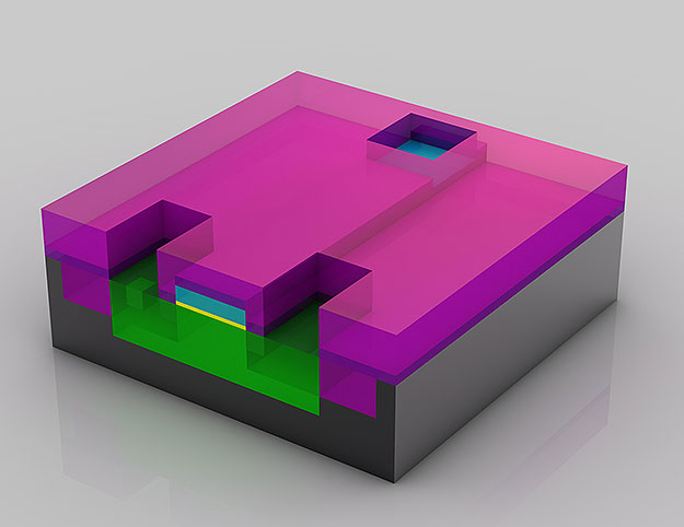
Electroplating the chip
Electroplating
scale: transistor level (~50-200 nm)
The wafers are put into a copper sulphate solution as this stage. The copper ions are deposited onto the transistor thru a process called electroplating. The copper ions travel from the positive terminal (anode) to the negative terminal (cathode) which is represented by the wafer.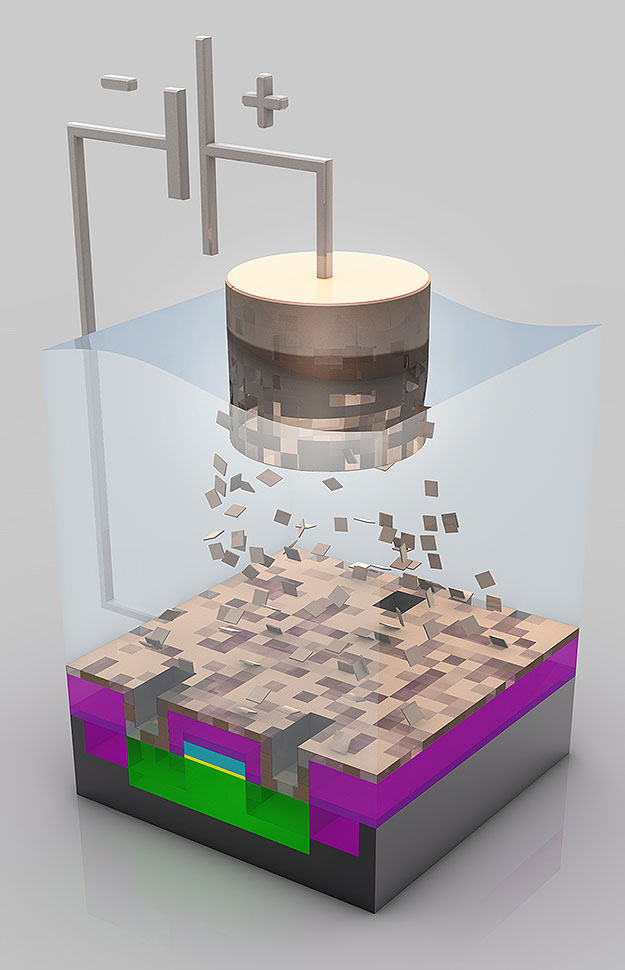
After Electroplating
scale: transistor level (~50-200 nm)
On the wafer surface the copper ions settle as a thin layer of copper.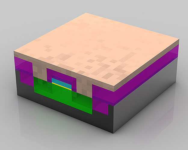
Polishing
scale: transistor level (~50-200 nm)
The excess material is polished off.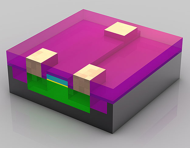
Adding metal layers
Metal Layers
scale: transistor level (six transistors combined ~500 nm)
Multiple metal layers are created to interconnect (think: wires) in between the various transistors. How these connections have to be "wired" is determined by the architecture and design teams that develop the functionality of the respective processor (e.g. Intel Core i7 Processor ). While computer chips look extremely flat, they may actually have over 20 layers to form complex circuitry. If you look at a magnified view of a chip, you will see an intricate network of circuit lines and transistors that look like a futuristic, multi-layered highway system.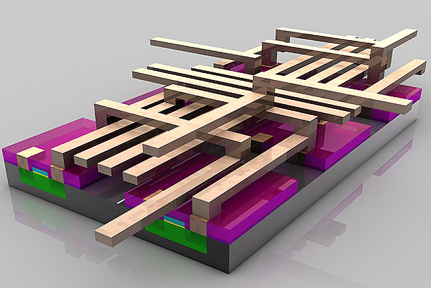
Wafer Sort Test
scale: die level (~10 mm / ~0.5 inch)
This fraction of a ready wafer is being put to a first functionality test. In this stage test patterns are fed into every single chip and the response from the chip monitored and compared to “the right answer”.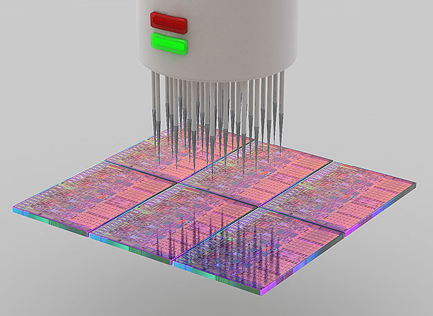
Wafer Sort Test
Wafer Slicing
scale: wafer level (~300 mm / 12 inch)
The wafer is cut into pieces (called dies).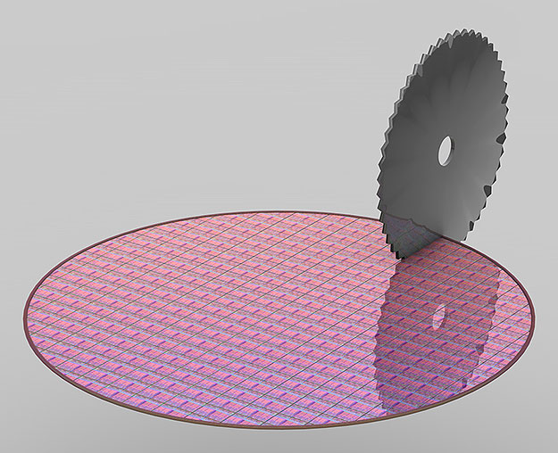
Chucking faulty chips
Discarding faulty dies
scale: wafer level (~300 mm / 12 inch)
The dies that responded with the right answer to the test pattern will be put forward for the next step (packaging).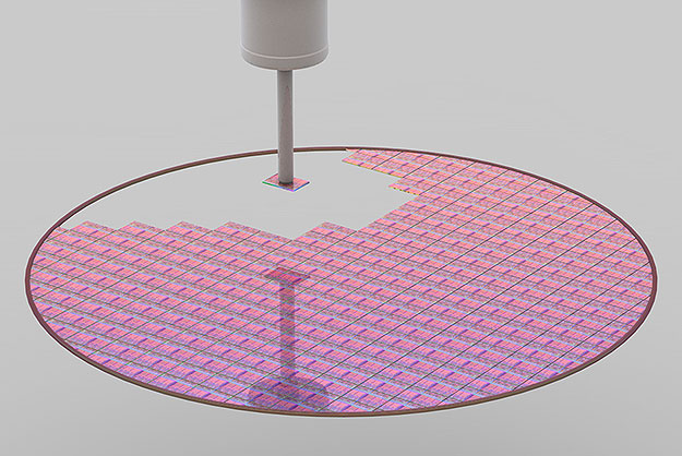
Individual Die
scale: die level (~10 mm / ~0.5 inch)
This is an individual die which has been cut out in the previous step (slicing). The die shown here is a die of an Intel Core i7 Processor .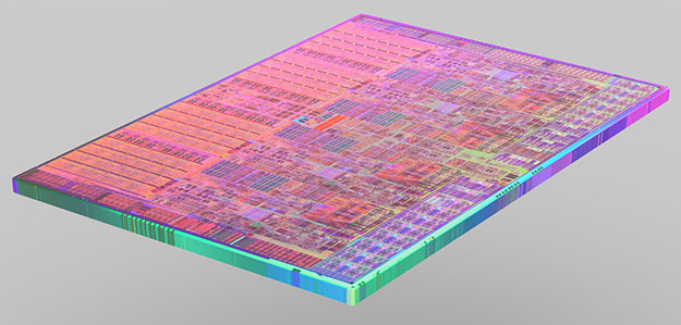
Packaging
scale: package level (~20 mm / ~1 inch)
The substrate, the die and the heatspreader are put together to form a completed processor. The green substrate builds the electrical and mechanical interface for the processor to interact with the rest of the PC system. The silver heatspreader is a thermal interface where a cooling solution will be put on to. This will keep the processor cool during operation.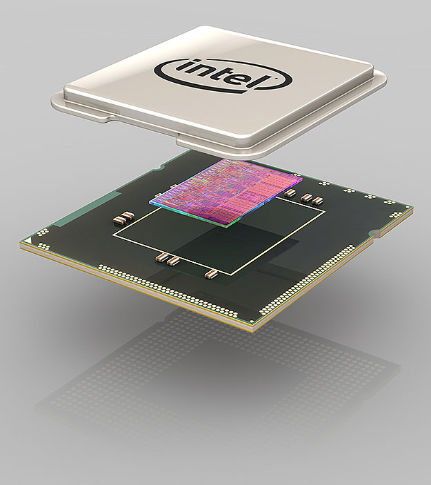
Packaging the chip
Processor
scale: package level (~20 mm / ~1 inch)
Completed processor (Intel Core i7 Processor in this case). A microprocessor is the most complex manufactured product on earth. In fact, it takes hundreds of steps — only the most important ones have been visualized in this picture story — in the world's cleanest environment (a microprocessor fab) to make microprocessors.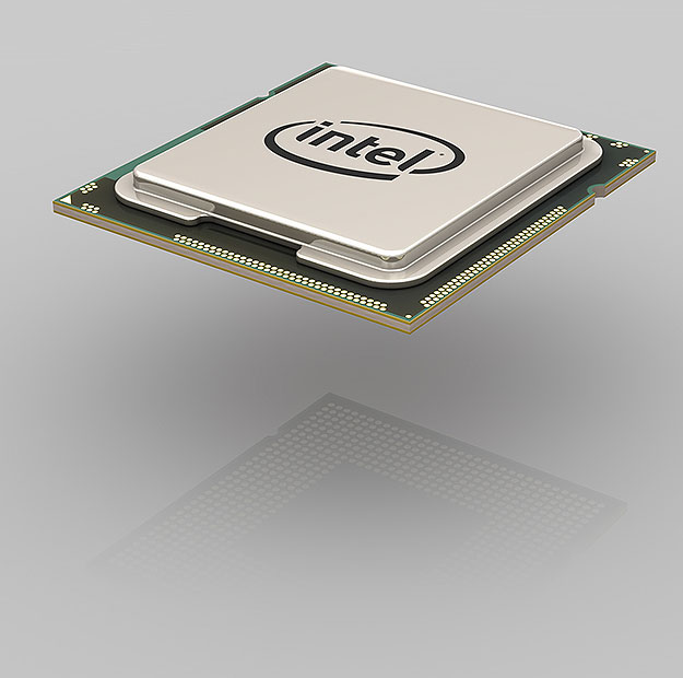
Class Testing
scale: package level (~20 mm / ~1 inch)
During this final test the processors will be tested for their key characteristics (among the tested characteristics are power dissipation and maximum frequency).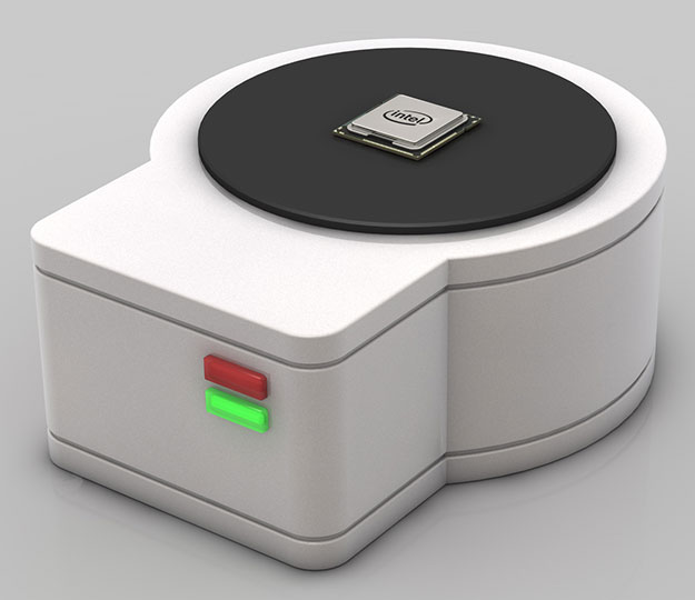
Binning
scale: package level (~20 mm / ~1 inch)
Based on the test result of class testing processors with the same capabilities are put into the same transporting trays.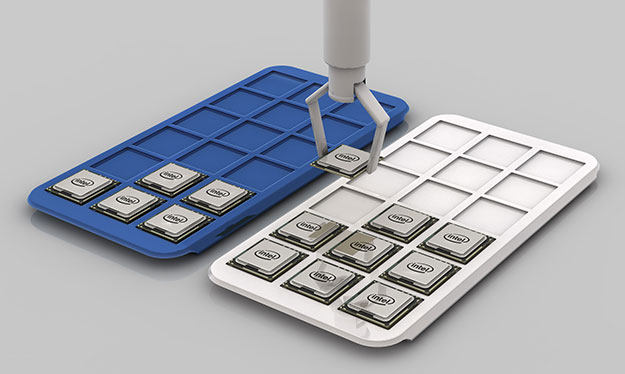
Finished product
Retail Package
scale: package level (~20 mm / ~1 inch)
The readily manufactured and tested processors (again Intel Core i7 Processor is shown here) either go to system manufacturers in trays or into retail stores in a box such as that shown here.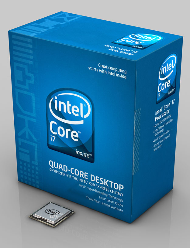
Images and explanatory text credit: Intel.